0
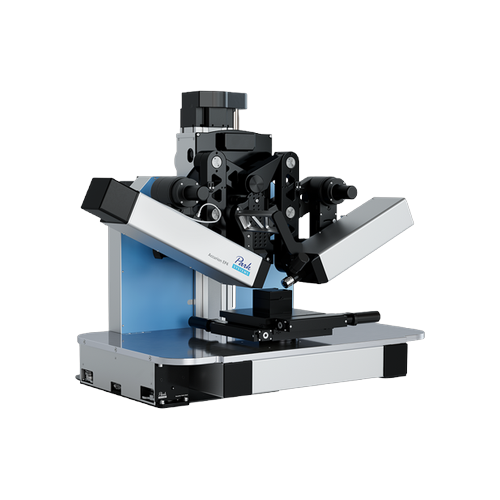
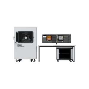
Park Systems Accurion EP4 이미징 타원편광분석기 Imaging Ellipsometer
Imaging ellipsometry combining microscopy and auto-nulling for 1 μm lateral resolution Delta/Psi mapping.
현미경과 자동 영점 조절 결합 이미징 타원편광분석기, 1μm 분해능 Delta/Psi 측정.
Description
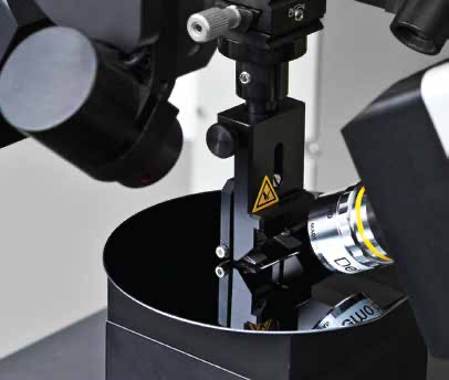
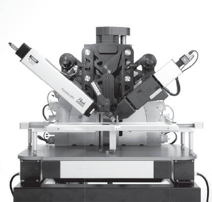
The Accurion EP4 is a well-established microscopic thin film, surface, and materials metrology tool generation that uses a combination of ellipsometry and microscopy to enable surface characterization with a lateral ellipsometric resolution down to 1 micron. This modular instrument enables configuration for your specific measurement tasks and offers a variety of unique features that allow the visualization of your surface in real time. You can measure parameters like thickness, refractive index, and absorption, and receive maps of selected areas.
It analyzes the change of polarization of light reflected from a sample and yields information about thin film layers that are often even thinner than the wavelength of the probing light itself. The enhanced lateral ellipsometric resolution is a result of the combination of a high numerical aperture objective that images about a million sites on the illuminated sample area onto a high-resolution 2-dimensional pixel detector-array.
Accurion EP4는 타원계측법(엘립소메트리)과 현미경 검사법을 결합하여 최대 1마이크론의 수평 타원계측 해상도로 표면 특성 분석을 가능하게 하는 미세 박막, 표면 및 재료 측정 장비 세대입니다. 이 모듈형 장비는 특정 측정 작업에 맞게 구성을 최적화할 수 있으며, 실시간으로 표면을 시각화할 수 있는 다양한 독특한 기능을 제공합니다. 두께, 굴절률, 흡수율과 같은 파라미터를 측정하고 선택한 영역의 맵을 얻을 수 있습니다.
이 기술은 시료에서 반사되는 빛의 편광 변화를 분석하여 조사하는 빛의 파장보다 더 얇은 박막 층에 대한 정보를 제공합니다. 향상된 수평 타원계측 해상도는 조명된 시료 영역의 약 100만 개 지점을 고해상도 2차원 픽셀 검출기 배열에 이미징하는 고개구율(high NA) 대물렌즈의 결합 덕분입니다.
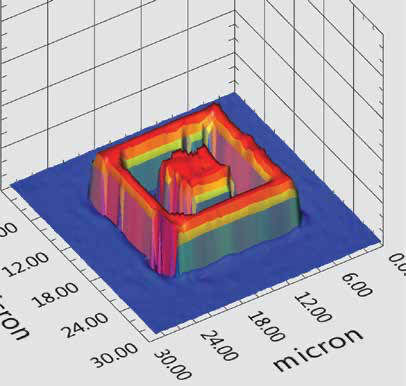
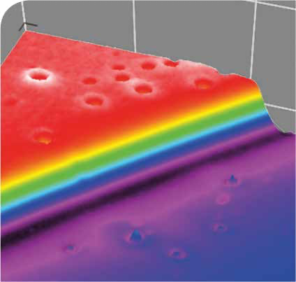
- Air | SiO 2 | Si Thickness map
- EP4 equipped with a UV and NIR camera
- The new adaption platform
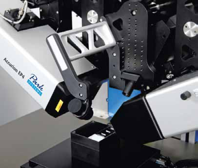
- EP4 beam cutter – a nondestructive way to eliminate backside reflection
- THE HIGHEST LATERAL ELLIPSOMETRIC RESOLUTION : The combination of microscopy and auto nulling ellipsometry allows a lateral ellipsometric resolution as small as 1 micron.
- IMAGING ELLIPSOMETRY IN THE WAVELENGTH RANGE OF 190 TO 2750 NM: With the use of a grating monochromator now continuous spectroscopic measurements are possible.
- TECHNOLOGY INTEGRATION PLATFORM: Implementation of complementary technologies e.g. Raman, AFM etc. provide even more information on your sample
- VARIOUS UNIQUE FEATURESA: variety of further new features and accessories enabling ellipsometry for new applications.
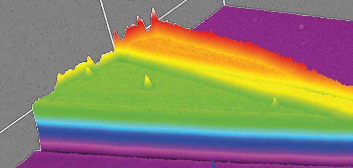
- Materials research example: graphene layer
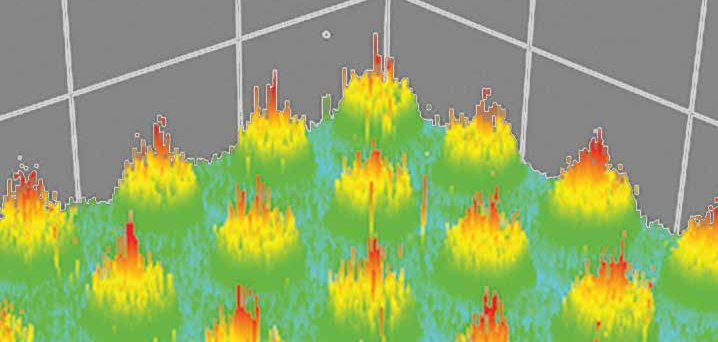
- Bio application example: protein spots on glass
Applications
- Graphene, 2D-Materials: Direct visualization of your 2D-material flakes on various substrates/materials; measuring thickness and optical properties of different 2D-material layers in the micrometer scale.
- Photonics, Displays, MEMS: Spectroscopic measurements on very small regions of only a few micron using the patented ROI (region of interest) concept to derive film thickness, refractive index, composition, and contaminations from a single measurement.
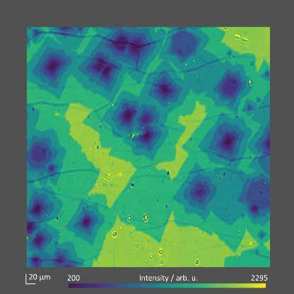
- Surface Engineering: Surface inspection of silanization patterns to form bonds across the interface or as the anchor for further steps of surface modifications.
- Air/Water or Liquid/Liquid Interface: Real-time visualization of Langmuir-Blodgett monolayers using Brewster angle/LIQUID microscopy (BAM).
- Bio Interfaces: High sensitivity observation for thickness or surface coverage of mono- as well as sub-monolayers with microscopic resolution, with a controllable environment to avoid damaging materials.
- Organic Electronics, Solar Cells: Determining optimal parameters and properties of thin conductive polymers for solar cells or OLEDs.
- Anisotropic Films: Modeling of refractive indices (uniaxial, biaxial) and the orientation of optical axes of anisotropic materials.
-
그래핀 및 2D 소재: 다양한 기판/소재 위에 있는 2D 소재 플레이크의 직접적인 시각화, 마이크로미터 스케일에서 서로 다른 2D 소재 층의 두께 및 광학적 특성 측정.
- 광학, 디스플레이, MEMS: 특허받은 ROI(관심 영역) 개념을 사용하여 단 몇 마이크론의 초미세 영역에 대한 분광 측정 수행, 단 한 번의 측정으로 박막 두께, 굴절률, 조성 및 오염 물질 도출.
- 표면 공학: 계면 간의 결합을 형성하거나 추가적인 표면 개질 단계의 앵커 역할을 하는 실란화 패턴의 표면 검사.
- 공기/물 또는 액체/액체 계면: 브루스터 각/액체 현미경 검사법(BAM)을 이용한 랭뮤어-블로젯(Langmuir-Blodgett) 단분자층의 실시간 시각화.
- 바이오 인터페이스: 관찰 대상 물질에 영향을 주거나 손상을 주지 않도록 환경 제어가 가능한 상태에서 미세 해상도로 단분자층 및 서브 단분자층의 두께 또는 표면 피복도를 고감도로 관찰.
- 유기 전자 장치, 태양 전지: 태양 전지나 OLED 분야에서 전도성 고분자의 특성을 이해하고 맞춤화하기 위한 최적의 파라미터 결정.
- 이방성 박막: 이방성 재료의 광학 축 방향 및 굴절률(단축, 쌍축) 모델링.
- Characterization of complex layer stack of a pixel in parallel including common layer stack modelling
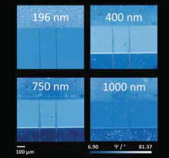
- Psi maps of linear waveguides, characterized at different wavelength making use of knife edge illumination
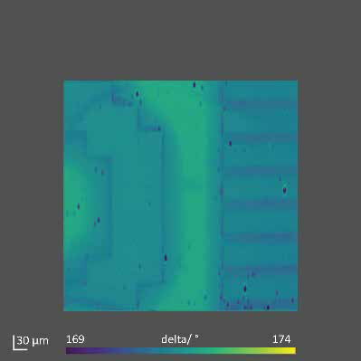
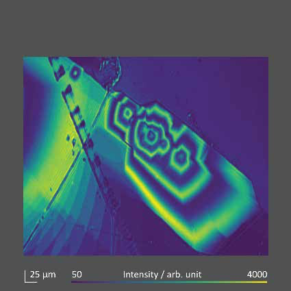
- Surface inspection of Silanisation pattern
- Air | Monopalmitoyl-rac-glycerol | water BAM image (180 Å2 /min · molecule)Air | Monopalmitoyl-rac-glycerol | water BAM image (180 Å2 /min · molecule)
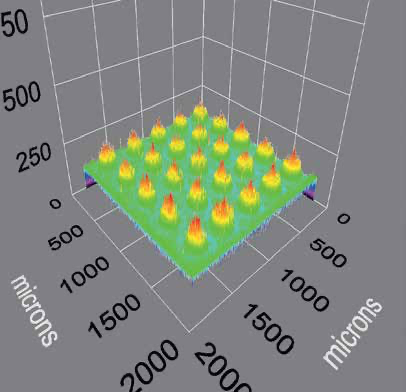
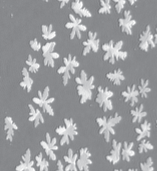
- Image scan of protein spots on glass
- Air | PCBM (spincoated) | Si-3D Delta map
- Air | Black Phosphorus | SiO 2 (300 nm) Si In-plane dispersion function
- EP4 beam cutter – a nondestructive way to eliminate backside reflection
Specifications
| Cameras | Technical description | What is it good for? |
|---|---|---|
| Standard cameraNew | High quality, monochrome GigE CCD cameraWavelength: 360-1000 mm1392 x 1040 pixel, 12 bits, max. 25 frames per second (fps) | Usually the CCD is used in 2x 2 binning mode to improve the signal and is operated at 20 fps. |
| OPTIONALNIR camera (only with IR upgrade) | InGaAs FPA, cooled, GigE interfareWavelength range: 900-1700 nm, 320 x 256 pixels, 25 fps fixed | • For spectroscopic measurements in the NIR this camera is added to the standard or the UV camera• Allows measurements eg for telecommunication materials. water absorption and many more. |
| OPTIONALUV camera (only with UV upgradel | Back-illuminated CMOSCameralink interfaceWavelength: 200-1000 tim, 1280 x 1040 pixels, 25 fps | For spectroscopic measurements in the UV. Camera will be operated in 2×2 hinning mode by default. This camera replaces the standard camera in all configurations that operate 360 om. The camera link interface board is included. |
| OPTIONALAdaption package for second camera | Switchable mirror or dichroic filter for camera selection (via software)Optical camera adaptation. Mechanical mounts | For broad range spectroscopy a secondary camera is being used. Optics for both cameras provide a similar, positionadjusted FOV. By this, seamless switching of the camera during spectral measurements is enabled |
| OPTIONALAlternative cameras | Any GeniCam-compatible camera (camera link board required) | The modular software concepts allow integration of various other cameras. Especially all GeniCam cameras are supported. Some cameras may require additional PC boards (camera link |
| Objective for use with focus scanner | Specification of the EP4, equipped with the following objectives: | What is it good for? |
|---|---|---|
| OPTIONAL2x objective | Lateral ellipsometric resolution: 10 μπιFOV: 2 mm x 2 mm, depends on AOI | Long distance objectives with high numerical apertures. |
| OPTIONAL5 x abjective | Lateral ellipsometric resolution: 4µmFOV: 800 μm 800 pm, depends on ADI | FOV (field of view) is based on standard camera, The FOV is quadratic for this camera at 42″ AOI. At different AOL, the FOV becomes rectangular depending on the angle. |
| ΟΡΠΩΝΑΙ10 x objective | Lateral ellipsometric resolution: 2 µmFOV: 400 um×400 v µm, depends on ADI | Resolution is defined at 400 nm. |
| OPTIONAL20 x objective | Lateral ellipsometric resolution: 1 μηFOV: 200 sim×200 µm, depends on ADI | Not applicable for UV |
| OPTIONAL50 objective | Lateral ellipsometric resolution: 1 µmFOV: 70 m˙×30 µm, depends on AQIOnly suitable for small samples (approx 70×20mml | Not applicable for UV |
| OPTIONALNanochromat | Lateral ellipsometric resolution: 2.5FOV: 600 µm x 600 pm, depends on ADI | UV/IR objective. Necessary for all measurements that include wavelength between 250 and 360 mm |
| Technical specification | Description |
|---|---|
| Ellipsometer Type | Brewster Angle Microscope (BAM)Imaging Elipsometer (IE) in PCSA configurationSpectroscopic Insaging Ellipsometer (SIE) in PCSA confi guration |
| Open Frame-Setup | Rugged aluminum frame construction with integrated multi-axis alignment.Separate electronic control sinit. |
| Imaging Optics | Automatic focus scanner for high-resolution, ellipsometric contrast images and maps, 10 objective (image width-400 µm, lateral resolution-2 µm(other objectives with larger field-of-view or higher lateral resolution are available)Ultraobjective for overall focused images (optional): 2 um lateral resolution, angle of incident range: 52-57 |
| Motonzed Goniometer | Patented software controlled motorized goniometer38−90∘ Angle-of-incidence rangeAngle resolution: 0.001Absolute angle accuracy: 0.01Speed of motion: –2.5/sec |
| X-Y Motorized Stage | 10 cm travel range, 1 um repeatability, 0.5 µm resolution |
| Electronics | Up-to-date monitor and Windows PCEmbedded Linux operating system (intermal only)Communication with host PC via dedicated 100 Mbit Ethernet |
| Power Supply | Voltage: 100-240 V, 50/60 Hz, max. current: 10 A |
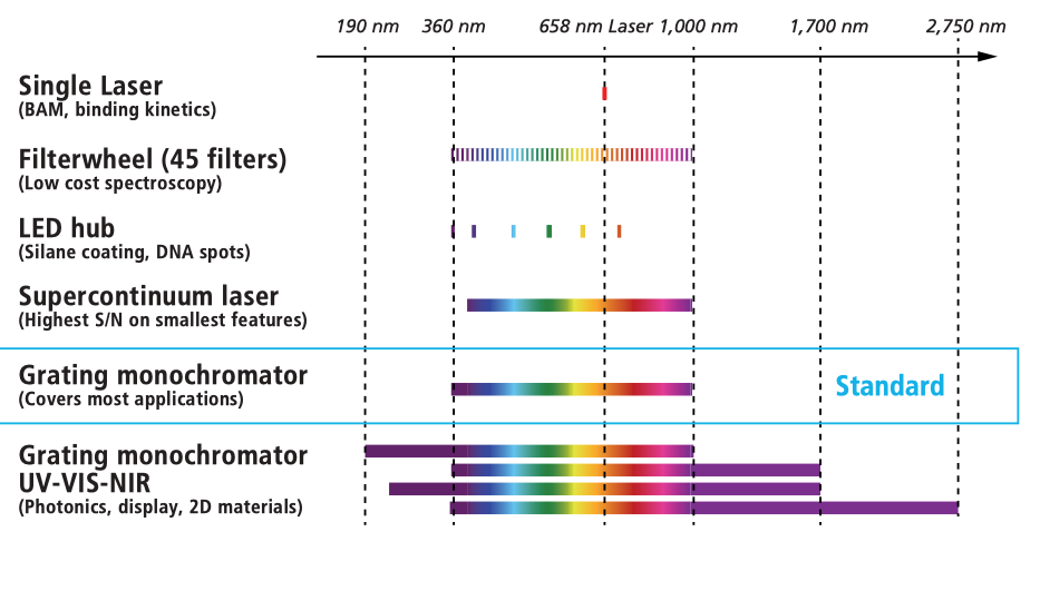
Options – Light Sources (combinations possible)
📎 원본 제품 페이지: https://www.parksystems.com/en/products/ellipsometers/imaging-spectroscopic-ellipsometry-