
Photoluminescence And Electroluminescence characteristics testing of InGaN/GaN Quantum Well
Introduction
Since the early 1990s, there has been a worldwide surge of interest in the development of high-brightness light-emitting diodes (LEDs), which has significantly advanced the field of solid-state lighting. High-brightness LEDs commonly adopt double heterostructures, necessitating excellent lattice matching between materials. This requirement imposes stringent limitations on the choice of semiconductor systems suitable for heterojunction LEDs.
Group III–V nitride semiconductors—such as AlN, GaN, and InN—have attracted considerable attention due to their superior optoelectronic properties and high chemical stability. These materials are capable of operating under extreme conditions, including high temperature, acidic or basic environments, and exposure to radiation. Additionally, their wide and tunable bandgap makes them ideal for high-power optoelectronic applications. By controlling the alloy composition, the bandgap can be continuously adjusted from 0.7 eV (InN) to 3.4 eV (GaN) and up to 6.2 eV (AlN), covering the entire visible spectrum and extending into the ultraviolet region. This makes them particularly suitable for high-brightness LED fabrication.
In this study, we evaluated the luminescence performance of InGaN/GaN multiple quantum wells at room temperature. The samples were grown on sapphire substrates via metal-organic chemical vapor deposition (MOCVD) and provided by King Abdullah University of Science and Technology.
Photoluminescence (PL) and electroluminescence (EL) measurements were conducted using the OmniPL Modular Measurement System developed by Zolix Instruments Co., Ltd.
Measurement Principle
When a semiconductor is irradiated with a light source whose photon energy exceeds the material’s bandgap, electrons in the valence band are excited to the conduction band, generating excess non-equilibrium carriers—electron-hole pairs. These carriers recombine through various mechanisms and emit photons. The emitted light is collected and directed into a monochromator for spectral dispersion, followed by detection and amplification using a photodetector. The resulting spectrum, which shows the photoluminescence intensity as a function of photon energy, reveals the material’s emission characteristics.
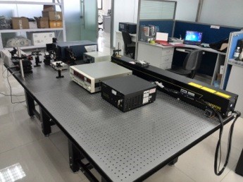
Experimental Setup
The OmniPL Modular System used for this study consists of the following components:
- 30 mW He-Cd laser (325 nm)
- Omni-λ500i imaging-corrected spectrometer
- Photomultiplier tube (PMT)
- Probe station and sample holder
For this experiment, a free-space optical path was configured according to user-specific requirements. The system also supports alternative configurations, such as microscope-based optics and low-temperature measurement modules.

Experimental Results
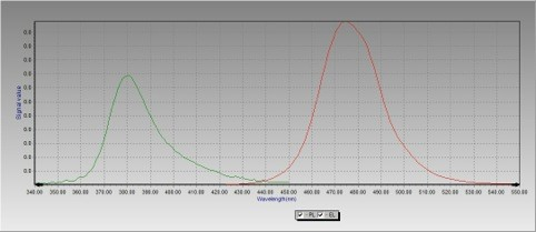
1. Photoluminescence (PL) Measurement
PL spectra were recorded by probing both the anode (red curve) and the cathode (green curve) of the sample. The intrinsic GaN emission peak was observed near 365 nm along with a characteristic yellow band. A strong InGaN emission peak was identified near 475 nm, indicating effective quantum well emission.
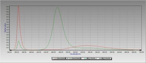
2. Electroluminescence (EL) Measurement
By applying a DC voltage of 2.5 V across the sample, a distinct blue electroluminescence was observed. The EL spectrum (red curve) showed a peak emission near 475 nm, consistent with the PL results. For comparison, the green curve in the figure represents the PL spectrum of a separate ZnO sample.
Conclusion
The OmniPL Modular Photoluminescence and Electroluminescence Measurement System offers a convenient and efficient platform for characterizing PL and EL properties of semiconductor materials. With options for free-space and microscope optics, low-temperature configurations, and PL mapping accessories, the system provides versatile functionality to support advanced research in InGaN/GaN quantum well structures. Its cost-effectiveness and adaptability make it a valuable tool for both academic and industrial applications.