

NIR Testing Techniques for MEMS Devices
Introduction:
In semiconductor manufacturing, fully automated wafer defect inspection during the early stages is critically important. In the backend process, multiple wafers are often bonded together or attached to opaque materials. Since semiconductor materials are opaque to visible light, it is difficult to characterize or inspect the bonding quality or contamination on bonding surfaces using visible imaging techniques. Near-infrared (NIR) inspection technology is an emerging and promising quality monitoring method in the semiconductor industry. This article focuses on the crucial role of near-infrared imaging inspection technology in MEMS industrial production.
Application in MEMS Sorting:
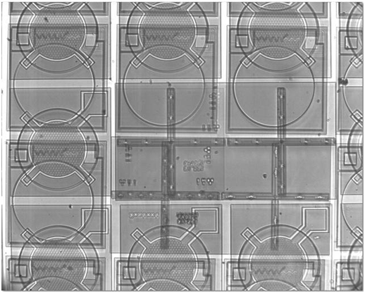
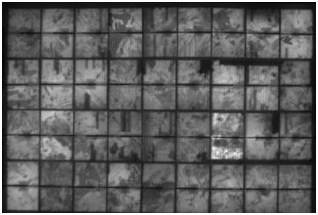
MEMS integrate micro-mechanical components, micro-sensors, and microelectronic circuits onto a single chip. To ensure MEMS functionality, defect inspection is essential. Many mechanical defects cannot be determined solely through electrical or functional testing. Such defects often occur on the substrate or bonding interfaces between the device and the capping wafer, making visible light imaging inadequate. Therefore, near-infrared inspection, as a non-destructive method, can detect defects on both upper and lower surfaces as well as internal defects within the device. Theoretically, this technology can detect all types of defects, including particles (contamination), etching lines, alignment marks, structural integrity, voids, and bonding process quality, among others.
Types of Defects and Detection Methods:
Experiments have shown that near-infrared inspection technology for MEMS devices can detect a range of important defects during MEMS production. Moreover, it can measure internal structures within bonded wafers.
Particles:
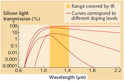
Particles can appear on the top surface, bottom surface, or between bonded wafers. The third scenario is the hardest to detect, as ultraviolet or visible light techniques only detect particles on the top or bottom surfaces. Infrared imaging can detect particles between wafers because silicon is transparent to infrared light; thus, particles appear as dark spots against a bright background. Some silicon fragments with inclined surfaces may produce similar effects but can be differentiated using specific algorithms.
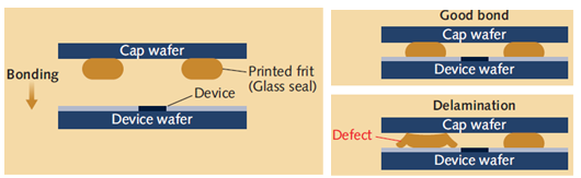
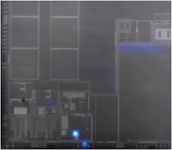
Eutectic/Melting Bonding Process:
In this bonding method, two wafers are directly bonded without any intermediate substrate. Such bonding rarely exhibits infiltration or exfiltration. Delamination is rare, but voids remain a critical factor. Precise localization of voids — including position, size, and thickness — allows identification of affected dies, preventing discarding entire wafers due to partial defects.
Sintering Defects:
During bonding using sintering, various defects may occur inside the solder material:
Etching Line Inspection:
Wet chemical etching requires wafers to be immersed in solutions, making it impractical to inspect every etching line. Sampling inspection manages the process quality. After etching and before bonding, sampling inspection achieves good resolution but requires expensive equipment. Etching line inspection measures line width, position, and spacing relative to other lines or alignment marks, which can be done alongside other infrared imaging inspections.
Alignment Mark Inspection:
Alignment marks exist on both devices and wafers and are typically checked before bonding. Though not usually re-checked, bonding misalignment can occur. Since near-infrared imaging penetrates both silicon layers, it can simultaneously detect absolute and relative positions of alignment marks to confirm bonding accuracy.
Macroscopic Structure Inspection:
Based on actual resolution, infrared inspection measures the chip’s active area macroscopic structures, typically with precision from 5 to 0.7 µm. While insufficient for detailed quality evaluation alone, it ensures no major macroscopic defects during the process stage. Used as a preliminary defect screening tool, it enhances system value.
Our MEMS Near-Infrared Inspection Technology:
We utilize narrowband near-infrared detection technology. The near-infrared wafer inspection system consists of a solid-state light source, infrared optical system, and high-speed, high-resolution near-infrared imaging sensor. With recent advances in solid-state infrared sources and sensor sensitivity, near-infrared imaging has become an effective method for detecting wafer defects.
Near-infrared inspection technology is a promising new approach in semiconductor quality control. It complements existing detection methods and offers new possibilities, especially for internal structure inspection. This non-destructive capability makes it especially valuable for MEMS devices. Hence, near-infrared imaging inspection plays a pivotal role in MEMS industrial production.
Near-Infrared Imaging Inspection Products:
Photonic Science SWIR Series Cameras (UK)
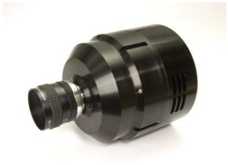
640×512 resolution InGaAs short-wave infrared cameras
Thermoelectric cooling
Cutoff wavelength at 1700 nm (extendable to 2200 nm)
Typical Applications:
MEMS device NIR transmission imaging inspection
Solar cell electroluminescence NIR inspection
Integrated circuit electroluminescence inspection