Description
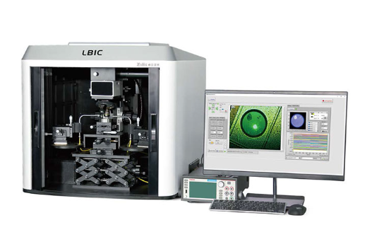
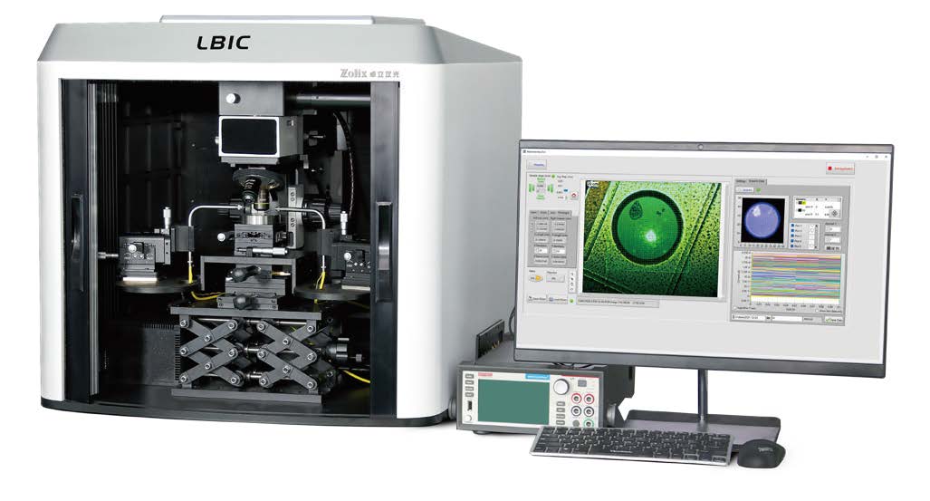
DSR500-LBIC Micronano Photoelectric Imaging Measurement System
Details
Product Instruction:
Micro-nano Photoelectric imaging measurement system uses microscopic imaging technique, multi excitation light paths, to provide stable, little size monochromatic light to a photovoltaic test device. Its functions are characterizing the short-circuit current distributions, surface defect, and reflectivity in electronic devices.
Based on the galvo scanning technique, the system features fast scanning and high spatial resolution, widely used to research solar cells and photoelectric devices, such as Dye sensitized, monocrystal silicon, multicrystal silicon, organic semiconductor, GaN detector, and so on. The photoelectric imaging can provide important analytic data for the QE, the resistance distribution, and the inhomogeneity of photo-generated current.
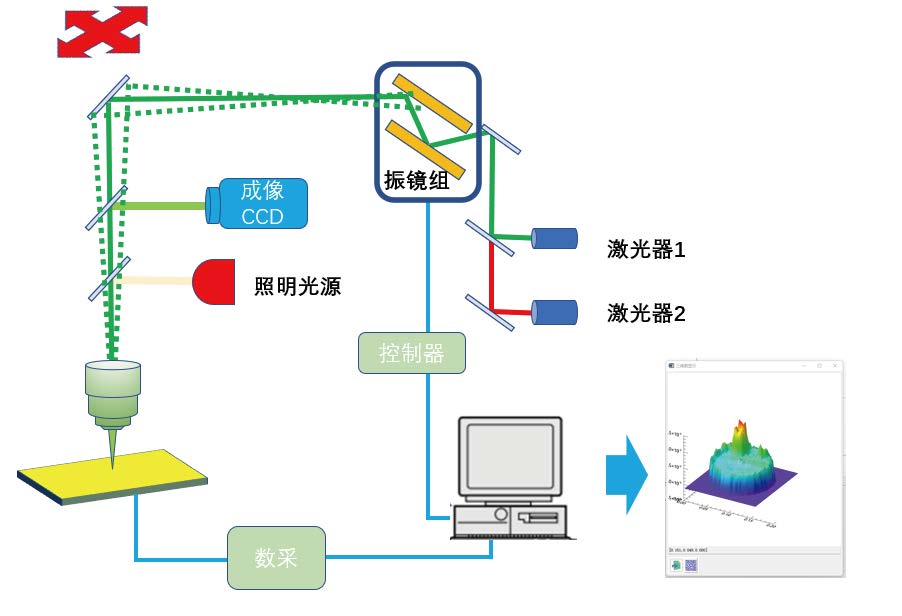
System Structure:
The system contains excitation lasers, scanning galvanometer, microscopy, data acquisition unit, and control software. When scanning the sample, the galvanometer make the laser spot scans and moves in the XY direction of the sample fast. The software records the position of each scanning point and current output value, and synchronously depicts a graph showing the current distribution of the sample. The light path also ensure the light spot pattern on different positions of the sample will not change.
Components:
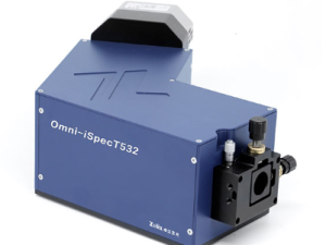
■ Light Sources
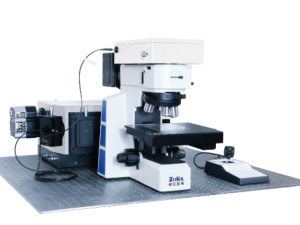
■ Microscopy
■ Scanning Galvanometer
■ Source Meter
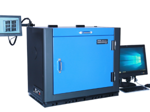
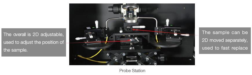
■ Probe Station and Software
Configuration:
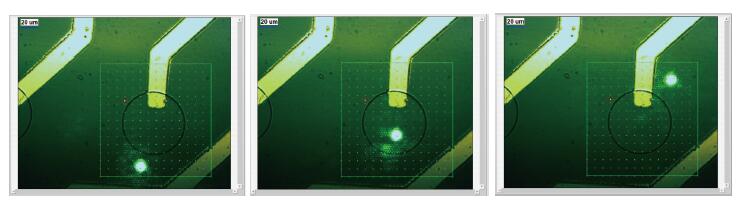
The spot modes at different positions of the setting area are same
Features
■ Multi-laser wavelength is optional
■ Easy sample replacement
■ XY linear stage is easy to change the measuring point of the sample
■ Galvo scanning removes the vibration effects
■ The visualization software can arbitrarily choose the scanning area
Applications:
Nanomaterials, 2D materials, Wafer Analysis, Detector Photoelectric Characteristic Test, Area Array Detector Pixel Measurement, Microdomain Characteristics of Device Charge Generation;
Specifications:
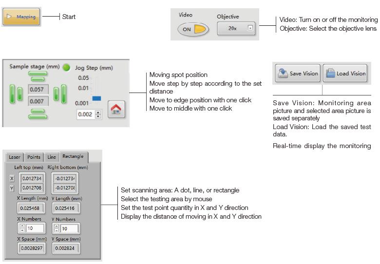
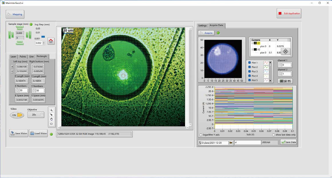
Software Function:
■ Move the position of the light spot
■ Select the testing area
■ Turn on/off the monitoring
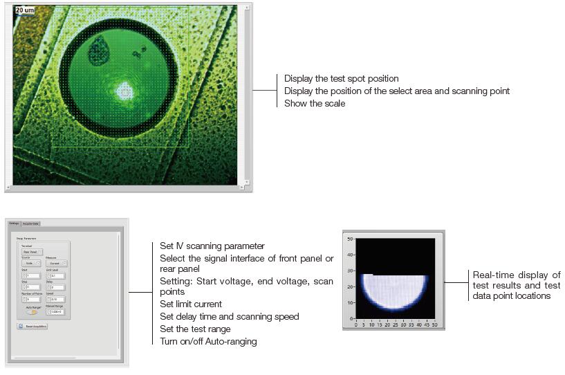
■ Set the parameter of the IV curve
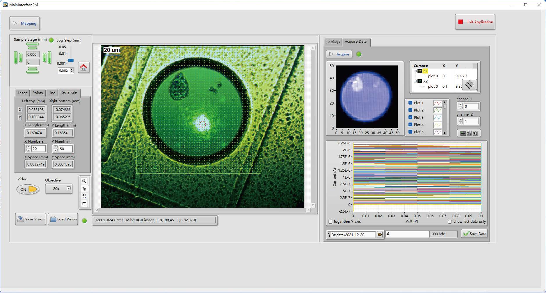
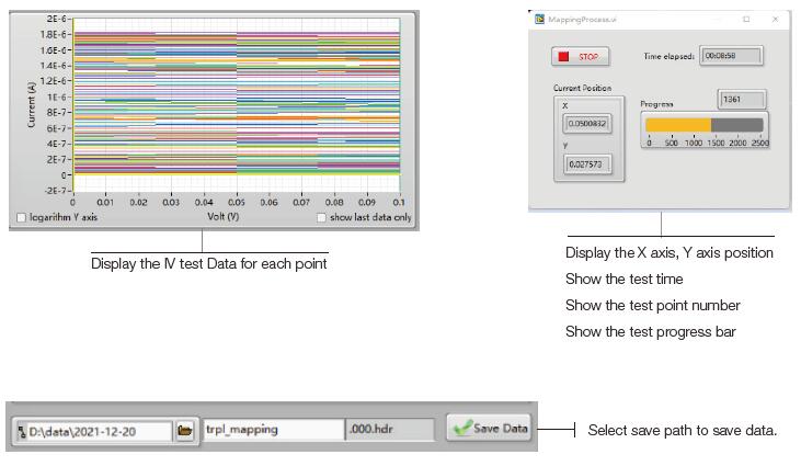
■ Real-time display of test data and test point locations
■ Display test progress and test time
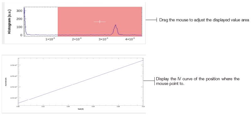
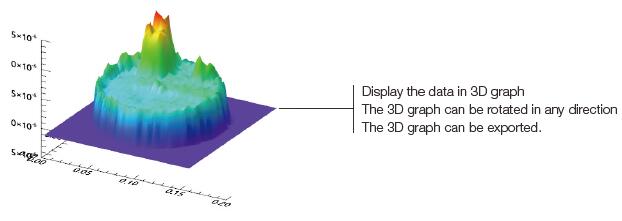
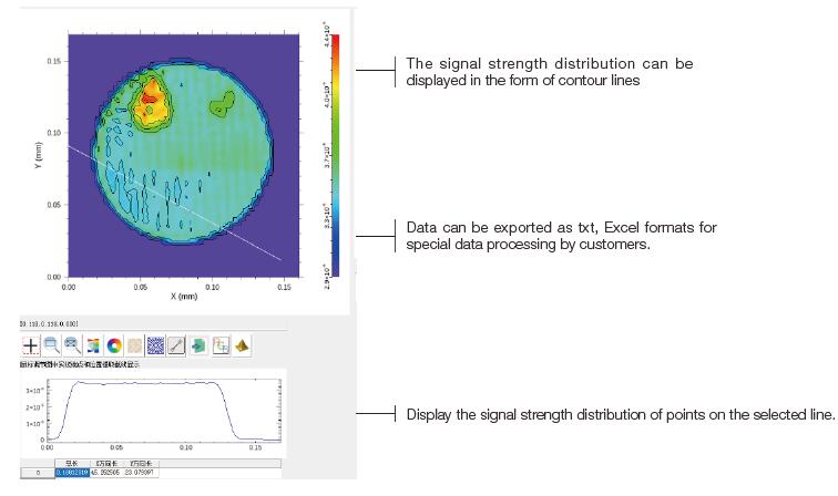
■ Data processing: thresholding, Zoom in or out, ascend line display, 3D data display, export data in txt or excel
Test sample diagram
Software interface:
Instruction of Software:
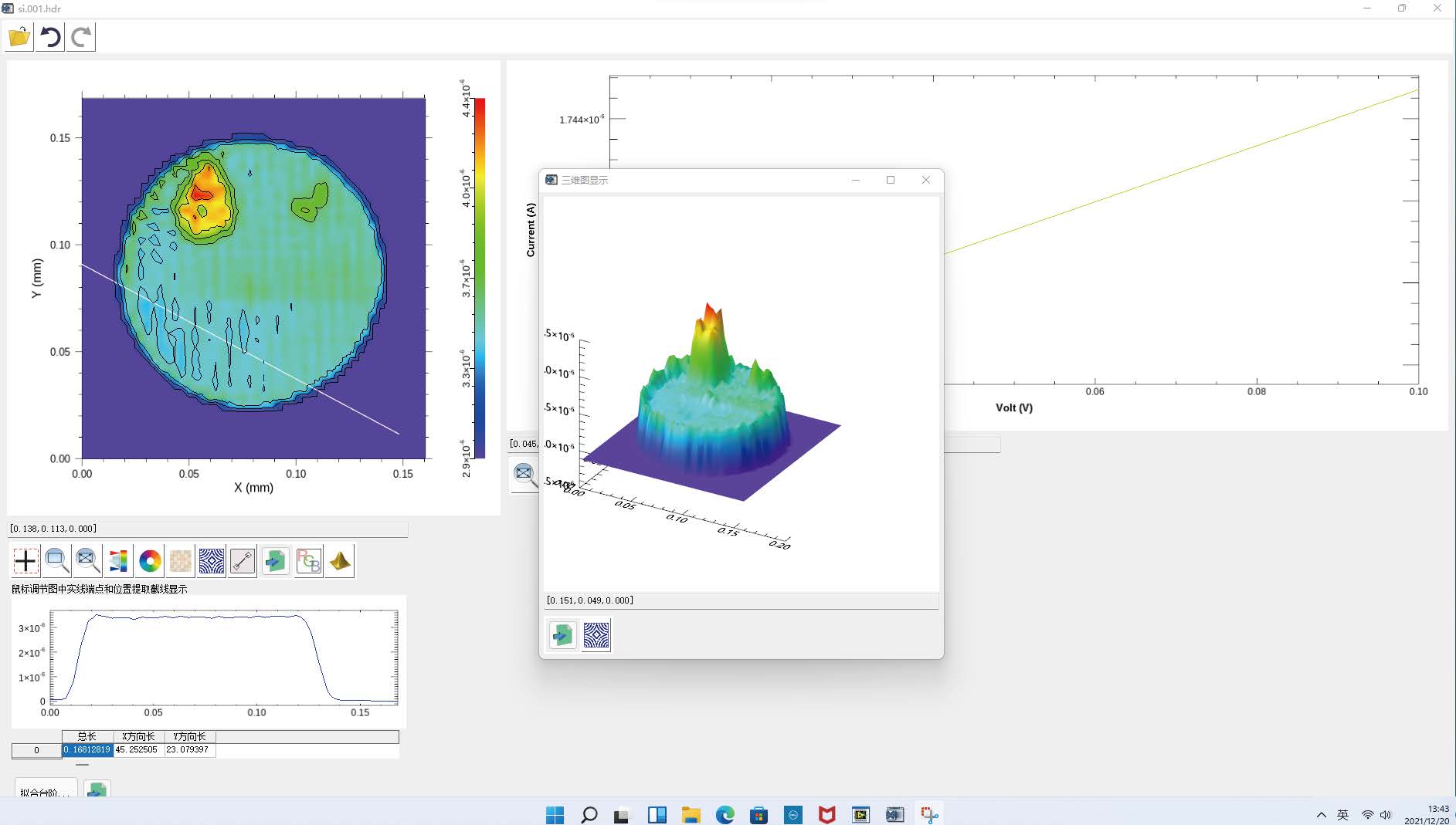
 The data analysis software shown as below:
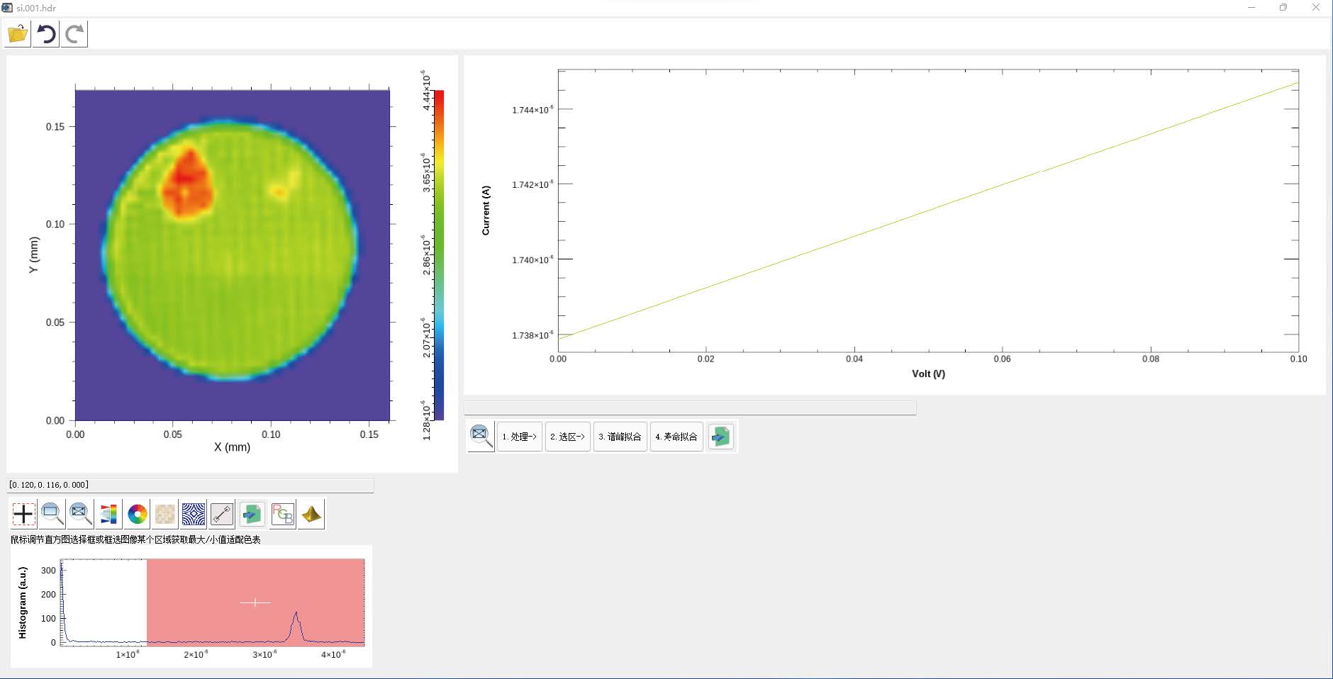
The analysis software feature powerful data processing functions, as shown in the picture below.
Examples:
1. Silicon detector: active area 120×120 μm
Test conditions:
■ Laser wavelength: 532nm;
■ Power: 1 mW
■ Objective Lens: 20 x.
Figure A, CCD monitoring graph of the sample scanning area; Figure B, contour map and 3D map of sample mapping data.
2. Nanomaterial-WSe2: active area 25×10 μm
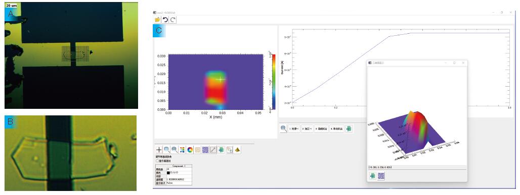
Figure A, the imaging map of the sample monitoring area, Figure B, the CCD monitoring map of the sample scanning area, Figure C, the sample scanning data contour map and 3D map.
Test conditions:
■ Laser wavelength: 532nm;
■ Power: 5 mW
■ Objective lens: 20 x.