0
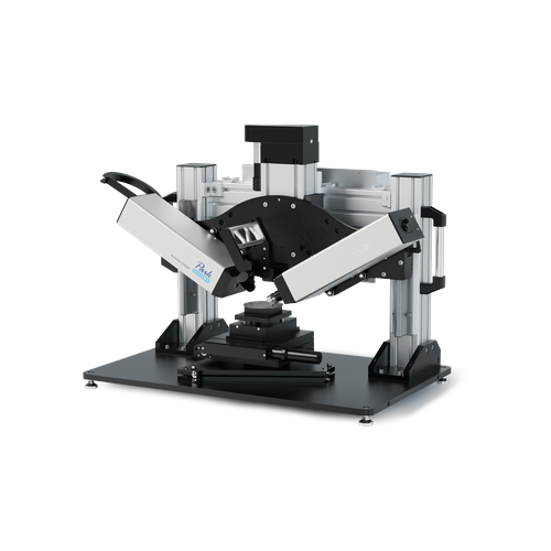
Park Systems Accurion SIMON 이미징 타원편광분석기 Imaging Ellipsometer
Entry-level imaging ellipsometer with fixed angle — fast surface inspection, thickness mapping, and 2D material flake search on large areas.
고정각 입문형 이미징 타원편광분석기, 대면적 표면 검사·박막 두께 매핑·2D 소재 플레이크 탐색.
Description
SIMON is specifically designed for routine measurement tasks. Its simple user interface and robustness of a fixed angle ellipsometer enables the entry to imaging ellipsometry. It can be operated in two different modes: the microscopic mode is very fast and allows visualisations of variations and defects in the thinnest layers (e.g., monolayers: d = 0.35 nm), whereas the ellipsometric mode measures thickness and the refractive index of the sample materials.
Imaging Ellipsometry itself combines the sensitivity of thickness and refractive index measurements with the imaging capabilities of microscopy, allowing for determining thickness and refractive index variations with microscopic images of micro-structured samples. Typical applications include the surface inspection of homogeneities and defects in large samples in quality control or the fast localization of flakes of 2D materials.
SIMON은 루틴 측정 작업을 위해 특별히 설계된 장비입니다. 간단한 사용자 인터페이스와 고정각 타원편광분석기의 견고성 덕분에 이미징 타원편광분석기의 입문 모델로 적합합니다. 두 가지 모드로 작동 가능합니다. 현미경 모드는 매우 빠르며 최박막(예: 단층막: d = 0.35 nm)의 변형 및 결함을 시각화하고, 타원편광 모드는 시료 물질의 두께와 굴절률을 측정합니다.
이미징 타원편광분석법은 두께·굴절률 측정의 민감도와 현미경의 이미징 능력을 결합하여, 마이크로 구조 시료의 현미경 이미지에서 두께·굴절률 분포를 결정할 수 있습니다. 대표적 응용으로는 품질 관리 시 대형 시료의 균질성·결함 표면 검사, 2D 소재 플레이크의 신속한 위치 탐색 등이 있습니다.

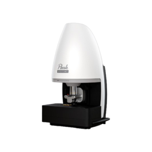
Accurion SIMON — compact fixed-angle imaging ellipsometer
Accurion SIMON — 컴팩트 고정각 이미징 타원편광분석기
Key Features
- Easy-to-use entry-level Imaging Ellipsometer — Simple user interface and robust fixed-angle design make imaging ellipsometry accessible for routine tasks and users new to the technique.
- Lateral ellipsometric resolution down to 1 µm — Imaging ellipsometry with micrometer-scale spatial resolution for micro-structured samples.
- Thickness and refractive index measurements of microstructures — Combination of ellipsometry and microscopy allows measurement of thickness maps comparable to AFM, including non-top layers.
- Large area inspection with automatic stitching — Designed to automatically stitch large areas with smooth transitions. A complete 4″ wafer can be inspected within 47 minutes, observing defects as small as 10 µm.
- Automatic flake search — Allows searching for flakes or materials with desired thicknesses; histogram analysis on a single measurement provides detailed distribution insights.
- Two operation modes — Microscopic mode: fast visualisation of layer thickness variations and defects / Ellipsometric mode: thickness and refractive index measurement.
- 사용하기 쉬운 입문형 이미징 타원편광분석기 — 간단한 사용자 인터페이스와 견고한 고정각 설계로 루틴 작업 및 처음 사용자도 이미징 타원편광분석법에 쉽게 접근 가능합니다.
- 1 µm까지의 측면 타원편광 분해능 — 마이크로 구조 시료에 대한 마이크로미터 스케일 공간 분해능을 갖춘 이미징 타원편광분석법.
- 마이크로구조 두께 및 굴절률 측정 — 타원편광분석법과 현미경의 결합으로 AFM과 유사한 두께 맵을 측정하며, 비상단 층도 측정 가능합니다.
- 자동 스티칭을 통한 대면적 검사 — 부드러운 전환으로 자동 스티칭 설계. 4″ 웨이퍼 전체를 47분 이내에 검사하며, 10 µm 크기의 결함도 관찰 가능.
- 자동 플레이크 탐색 — 원하는 두께의 플레이크나 소재를 자동으로 탐색. 단일 측정의 히스토그램 분석으로 두께 분포에 대한 상세한 통찰 제공.
- 두 가지 작동 모드 — 현미경 모드: 층 두께 변화 및 결함 신속 시각화 / 타원편광 모드: 두께 및 굴절률 측정.
Applications
- Large area surface inspection — quality control of thin film homogeneity and defects
- 2D materials — automatic flake search for graphene, MoS₂, hBN
- Thickness mapping of microstructures (comparable to AFM)
- Refractive index variation visualization (e.g., holographic gratings, waveguides)
- Monolayer detection (d = 0.35 nm)
- 대면적 표면 검사 — 박막 균질성 및 결함 품질 관리
- 2D 소재 — 그래핀, MoS₂, hBN 플레이크 자동 탐색
- 마이크로구조 두께 매핑 (AFM과 유사)
- 굴절률 분포 시각화 (예: 홀로그래픽 격자, 도파관)
- 단층막 검출 (d = 0.35 nm)
Specifications
Accurion SIMON의 주요 사양입니다. 자세한 사양은 견적 요청 시 안내드립니다.
| Parameter | Specification |
|---|---|
| Imaging | |
| Lateral ellipsometric resolution | Down to 1 µm |
| Field of view (single measurement) | Approx. 500 µm (X) × 550 µm (Y) |
| Measurement time (single field) | < 1 minute |
| Large area stitching — 4″ wafer | Within 47 minutes |
| Minimum detectable feature | 10 µm (defects / inhomogeneities) |
| Measurement | |
| Thickness resolution | < 0.01 nm |
| Thickness range | 0.01 nm – 5 µm (sample dependent) |
| Minimum detectable layer | Monolayer (d = 0.35 nm) |
| Angle of incidence | Fixed angle |
| Operation Modes | |
| Microscopic mode | Fast visualization of thickness variations and defects |
| Ellipsometric mode | Thickness and refractive index measurement |
| Sample | |
| Sample type | Wafers, large samples, microstructures, 2D materials |
| Large area inspection | Automatic stitching with smooth transitions |
📎 원본 제품 페이지: https://www.parksystems.com/en/products/ellipsometers/imaging-spectroscopic-ellipsometry-