0
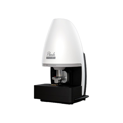
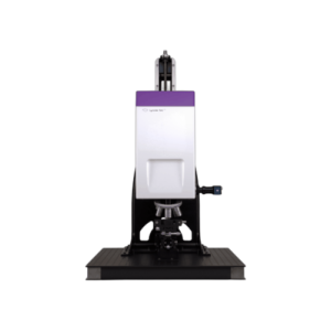
Park Systems FX40 원자현미경 AFM
High-resolution small sample AFM with low noise, automated probe exchange, laser alignment, Non-contact™.
고분해능 소형 시료 원자현미경, 자동 프로브 교환, 레이저 정렬, 비접촉 모드.
Description
Park FX40 is an innovative Atomic Force Microscope (AFM) designed for high-resolution imaging of small samples. Featuring a low noise floor, minimized thermal drift, and enhanced mechanical stability, the FX40 delivers the highest precision and reliability. Like all Park AFM instruments, the FX40 incorporates an orthogonal scan system and True Non-contact™ mode, enabling accurate high-resolution measurements even on fragile samples.
Park FX40은 소형 시료의 고해상도 이미징을 위해 설계된 파크시스템스의 혁신적인 원자력 현미경(AFM)입니다. 낮은 잡음 수준(noise floor), 최소화된 열 드리프트, 향상된 기계적 안정성을 바탕으로 최고의 정밀도와 신뢰성을 제공합니다. 모든 Park AFM 제품과 마찬가지로 FX40은 직교 스캔 시스템과 True Non-contact™ 모드를 탑재하여, 손상되기 쉬운 시료에서도 정확한 고해상도 측정이 가능합니다.
- Low noise floor with minimized thermal drift and enhanced mechanical stability
- Orthogonal scan system with True Non-contact™ mode for precise nanoscale imaging
- Automated probe exchange with kinematic mounting and QR-coded chip carriers
- Vision-based automatic laser beam alignment with PSPD auto-centering
- Sample view camera with one-click XY stage navigation
- Improved coaxial optical system for unobstructed field of view down to 0.87 μm line width
- Powerful FX AFM controller with 8-channel lock-in amplifier and 5 MHz bandwidth
- Fiber-coupled laser (SLD) integrated into optical microscope for minimized beam spot size
- Automatic Tip eXchanger (ATX) module supporting up to 8 pre-loaded probes
- 최소화된 열 드리프트 및 향상된 기계적 안정성을 갖춘 낮은 잡음 수준
- 정밀한 나노스케일 이미징을 위한 직교 스캔 시스템 및 True Non-contact™ 모드
- 키네마틱 마운팅과 QR 코드 칩 캐리어를 적용한 자동 프로브 교체
- PSPD 자동 중심 맞춤 기능이 결합된 비전 기반 레이저 빔 자동 정렬
- 원클릭 XY 스테이지 이동이 가능한 시료 관찰 카메라
- 0.87 μm 선폭까지 확인 가능한 동축 광학 시스템
- 8채널 록인 증폭기 및 5 MHz 대역폭을 갖춘 강력한 FX AFM 컨트롤러
- 빔 스폿 크기 최소화를 위한 광학 현미경 통합 광섬유 결합 레이저(SLD)
- 최대 8개의 프로브을 사전 장착할 수 있는 자동 프로브 교환기(ATX) 모듈
Applications
- High-resolution topographic imaging of small and fragile samples
- 2D material characterization (e.g. twisted bilayer graphene on hBN)
- Conductive AFM measurements (e.g. WTe₂ on Au electrode)
- Block copolymer and polymer composite nanoscale imaging
- Thin film surface analysis
- Life science nanoscale surface measurement
- Advanced electrical, mechanical, and thermal property analysis
- 소형 및 손상되기 쉬운 시료의 고분해능 형상 이미징
- 2차원(2D) 소재 특성 분석 (예: hBN 위 이중층 꼬임 그래핀)
- 전도성 AFM 측정 (예: Au 전극 위 WTe₂)
- 블록 공중합체 및 고분자 복합재의 나노스케일 이미징
- 박막 표면 분석
- 생명과학 분야 나노스케일 표면 측정
- 전기적, 나노역학적, 열적 특성 분석
Specifications
| AFM Modes |
|---|
| Standard |
| True Non-Contact™ |
| Contact AFM |
| Lateral Force Microscopy (LFM) |
| Phase Imaging |
| Tapping Mode |
| Force Distance (F/d) Spectroscopy |
| PinPoint™ AFM |
| Electrical |
| Conductive AFM (C-AFM) |
| IV Spectroscopy |
| Kelvin Probe Force Microscopy (KPFM) |
| Scanning Capacitance Microscopy (SCM) |
| Scanning Spreading-Resistance Microscopy (SSRM) |
| Scanning Tunneling Microscopy (STM) |
| Photo Current Mapping (PCM) |
| Electrochemical AFM (EC-AFM) |
| Thermal Stages (Optional) |
| Stage 1: -25°C to +170°C |
| Stage 2: Ambient to +250°C |
| Stage 3: Ambient to +600°C |

📎 원본 제품 페이지: https://www.parksystems.com/products/small-sample-afm/park-fx40