0
Park_AFM-IR Spectrometer_(FX40 IR / FX200 IR / FX300 IR)
Advanced nanoscale IR spectroscopy platform integrating AFM with Photo-induced Force Microscopy (PiFM) for simultaneous chemical composition and surface morphology analysis at sub-5nm spatial resolution.
Description
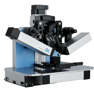
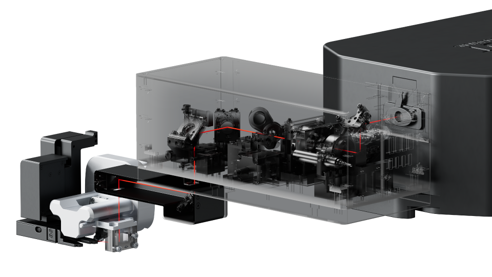
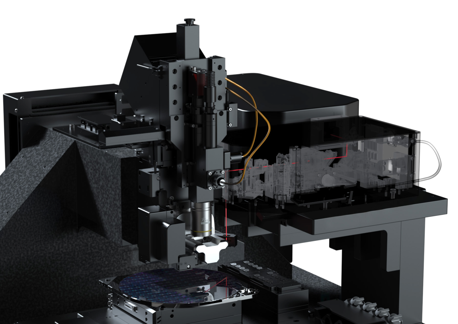
Park AFM-IR Spectrometer is an integrated platform combining Atomic Force Microscopy (AFM) with Photo-induced Force Microscopy (PiFM) technology. This innovative platform maintains full AFM functionality while providing nanoscale molecular vibration mapping, enabling comprehensive analysis of surface morphology, nanomechanical, electrical, and thermal properties. With PiFM mode, chemical composition and surface morphology can be analyzed simultaneously, making it ideal for nanoscale IR spectroscopy and imaging of semiconductors, polymers, thin films, 2D materials, and other advanced materials.
Park AFM-IR Spectrometer는 원자력 현미경(AFM)과 광유도력 현미경(PiFM) 기술을 통합한 분석 플랫폼입니다. 이 혁신적인 플랫폼은 AFM 기능을 유지하면서 나노스케일 분자 진동 매핑을 제공하여, 표면 형상, 나노역학적, 전기적, 열적 특성을 종합적으로 분석할 수 있습니다. PiFM 모드를 통해 화학 조성과 표면 형상을 동시에 분석할 수 있어 반도체, 고분자, 박막, 2차원(2D) 소재 및 기타 첨단 소재의 나노스케일 IR 분광 및 이미징에 적합합니다.
- High spatial resolution chemical imaging with sub-5nm spatial resolution and monolayer sensitivity
- True Non-contact™ IR measurement with PiFM — eliminates sample damage and tip contamination
- Comprehensive material characterization including surface morphology, nanomechanical, electrical, and thermal properties
- Automated IR laser alignment via SmartScan™ for minimal user intervention
- SmartAnalysis™ for advanced spectral visualization and chemical distribution map overlay
- Two smart detection modes: Direct Mode and Sideband Mode optimized for different sample characteristics
- Automated probe exchange and vision-based AFM laser beam alignment based on proven FX platform
- Orthogonal scan system with True Non-contact™ mode
- Resonance frequency optimization per pixel for stable, artifact-free PiFM imaging
- Compatible with KLARF file integration for defect-position-guided precision analysis
- High spectral correlation with conventional FT-IR spectroscopy results
- 5 nm 이하의 공간 분해능 및 단분자층 민감도를 갖춘 고분해능 화학 이미징
- PiFM 기반 True Non-contact™ IR 측정 — 시료 손상 및 탐침 오염 원천 방지
- 표면 형상, 나노역학적, 전기적, 열적 특성을 포함한 포괄적 소재 특성 분석
- 최소한의 사용자 개입을 위한 SmartScan™ IR 레이저 자동 정렬
- SmartAnalysis™를 통한 스펙트럼 시각화 및 화학 분포도 오버레이
- 시료 특성에 따라 최적화된 직접 모드(Direct Mode) 및 측파대 모드(Sideband Mode)의 두 가지 스마트 감지 모드
- 검증된 FX 플랫폼 기반의 자동 탐침 교체 및 비전 기반 AFM 레이저 빔 자동 정렬
- True Non-contact™ 모드를 갖춘 직교 스캔 시스템
- 안정적이고 아티팩트 없는 PiFM 이미징을 위한 픽셀별 공진 주파수 최적화
- 결함 위치 기반 정밀 분석을 위한 KLARF 파일 통합 지원
- 기존 푸리에 변환 적외선 분광법(FT-IR)과의 높은 스펙트럼 일치성
Applications
- Semiconductor defect analysis and process monitoring — precise nanoscale chemical identification of contamination, residues, and process anomalies with KLARF file integration
- Polymer and thin film nanoscale IR spectroscopy and imaging
- 2D material and advanced materials characterization
- Chemical distribution mapping of heterogeneous surfaces
- Nanoscale identification of contaminants and residues (e.g. PTFE, organic films)
- Life science and biomedical nanoscale surface analysis
- Nanoscale IR spectroscopy of block copolymer systems such as PS-b-PMMA
- Point spectroscopy and chemical imaging for material identification at specific sample locations
- Spectral-spatial correlation analysis
- 반도체 결함 분석 및 공정 모니터링 — KLARF 파일 통합을 통한 오염, 잔류물, 공정 이상의 나노스케일 정밀 화학 동정
- 고분자 및 박막의 나노스케일 IR 분광 및 이미징
- 2차원(2D) 소재 및 첨단 소재 특성 분석
- 불균질 표면의 화학 분포도 매핑
- 나노스케일 오염물 및 잔류물 동정 (예: PTFE, 유기 박막)
- 생명과학 및 생의공학 분야 나노스케일 표면 분석
- PS-b-PMMA 등 블록 공중합체 시스템의 나노스케일 IR 분광
- 특정 시료 위치에서의 점 분광 및 화학 이미징을 통한 물질 동정
- 스펙트럼-공간 상관 분석
Specifications
● Standard ○ Option – Not supported
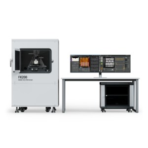
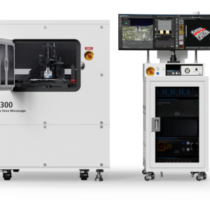
| Parameter | FX40 IR | FX200 IR | FX300 IR |
|---|---|---|---|
| QCL Laser (3 modules) | ● | ● | ● |
| Extended QCL Laser (4 modules) | – | ○ | ○ |
| QCL + OPO Laser | – | ○ | ○ |
| QCL + OPO/DFG Laser | – | ○ | ○ |
| Facility Controller | ○ | ● | ● |
| XEA Software | – | ○ | ○ |
| KnowItAll Software | ○ | ○ | ○ |
| Acoustic Enclosure Outer (W×D×H mm) | 970 × 990 × 1,530 | 1,250 × 1,280 × 1,570 | 1,250 × 1,280 × 1,570 |
| Cabinet (W×D×H mm) | 1,200 × 900 × 1,700 | 1,200 × 900 × 1,890 | 1,200 × 900 × 1,890 |
| Total Weight (AFM Body + AE) | 920 kg | 2,290 kg | 2,340 kg |
| Acoustic Noise Level | 65 dB | 65 dB | 65 dB |
| Floor Vibration Level | VC-D (6.25 µm/sec) | VC-D (6.25 µm/sec) | VC-D (6.25 µm/sec) |
| Power | 2.3 kW (Max) | 2.3 kW (Max) | 2.3 kW (Max) |