0
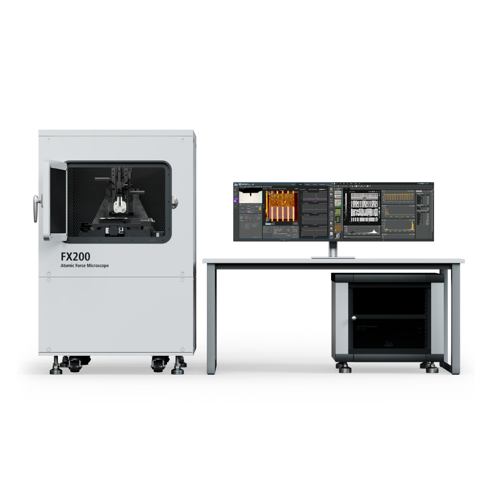
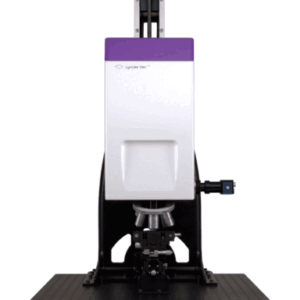
Park_FX200_(200 mm Sample AFM)
High-performance AFM optimized for 200 mm sample measurement, featuring low noise floor, minimized thermal drift, dual-servo XY scanner, automated probe exchange, and True Non-contact™ mode for precise nanoscale imaging across research and industrial applications.
Description
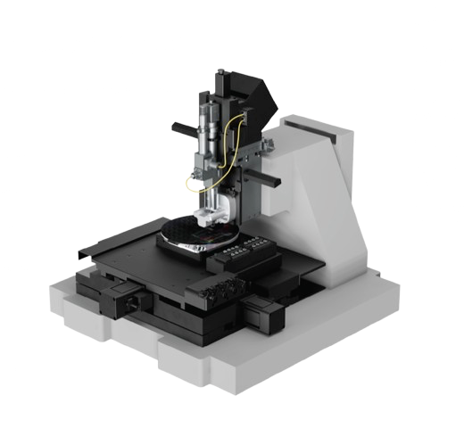
Park FX200 is an innovative Atomic Force Microscope (AFM) designed for measurements of samples up to 200 mm, offering the highest precision and reliability through a low noise floor, minimized thermal drift, and enhanced mechanical stability. Like all Park AFM instruments, the FX200 incorporates an orthogonal scan system and True Non-contact™ mode, enabling accurate high-resolution measurements even on fragile samples. Key features of the FX200 include automated probe exchange, laser beam auto-alignment, and a sample view camera capable of displaying the entire 200 mm sample. Additional capabilities such as automatic scan parameter optimization, optical autofocus, sequential multi-position measurement, and powerful data analysis tools enable complex tasks to be performed with ease. With advanced features and a user-friendly interface, the FX200 is the optimal solution for nanoscale imaging and analysis across research and industrial environments.
Park FX200은 최대 200 mm 샘플을 측정할 수 있도록 설계된 파크시스템스의 혁신적인 원자력 현미경(AFM)입니다. 낮은 잡음 수준(noise floor), 최소화된 열 드리프트, 기계적 안정성 향상을 통해 최고의 정밀도와 신뢰성을 제공합니다. 모든 Park AFM 제품과 마찬가지로 FX200은 직교 스캔 시스템과 True Non-contact™ 모드를 탑재하고 있어, 손상되기 쉬운 샘플에서도 정확한 고해상도 측정이 가능합니다. FX200의 주요 기능으로는 자동 프로브 교환, 레이저 빔 자동 정렬, 200 mm 샘플 전체를 확인할 수 있는 샘플 뷰 카메라 등이 있습니다. 자동 스캔 파라미터 최적화, 광학 오토포커스, 다중 위치에서의 순차 측정, 강력한 데이터 분석 도구 등의 추가 기능을 통해 복잡한 작업도 간편하게 수행할 수 있습니다. 첨단 기능과 사용자 친화적 인터페이스를 갖춘 FX200은 연구 및 산업 환경 전반에 걸쳐 나노스케일 이미징 및 분석에 최적화된 솔루션입니다.
- Low noise floor with minimized thermal drift and enhanced mechanical stability
- Orthogonal scan system with True Non-contact™ mode for precise nanoscale imaging
- Dual-servo XY scanner architecture for accurate full-area positioning on 200 mm samples
- Automated probe exchange with kinematic mounting and QR-coded chip carriers (up to 16 probes)
- Vision-based automatic laser beam alignment with PSPD auto-centering
- Sample view camera with full 200 mm wafer overview and one-click XY stage navigation
- Improved coaxial optical system for unobstructed field of view down to 0.87 μm line width
- Ultra-low Z-axis detector noise below 0.02 nm (rms), enabling sub-nanometer height measurement
- Powerful FX AFM controller with 8-channel lock-in amplifier and 5 MHz bandwidth tip bias modulation
- Upgraded active vibration isolation system with dual-layer base frame for dramatically reduced noise floor
- Live monitoring camera for real-time interior observation with enclosure door closed
- Park SmartScan™ with automated scan parameter optimization for ease of use
- Park SmartAnalysis™ for comprehensive AFM data analysis and workflow optimization
- 최소화된 열 드리프트 및 향상된 기계적 안정성을 갖춘 낮은 잡음 수준
- 정밀한 나노스케일 이미징을 위한 직교 스캔 시스템 및 True Non-contact™ 모드
- 200 mm 샘플 전체 영역에서 정확한 위치 지정을 위한 듀얼 서보 XY 스캐너 구조
- 키네마틱 마운팅과 QR 코드 칩 캐리어를 적용한 자동 프로브 교환 (최대 16개)
- PSPD 자동 중심 맞춤 기능이 결합된 비전 기반 레이저 빔 자동 정렬
- 200 mm 웨이퍼 전체 개요 확인 및 원클릭 XY 스테이지 이동이 가능한 샘플 뷰 카메라
- 0.87 μm 라인 폭까지 확인 가능한 개선된 동축 광학 시스템
- 0.02 nm (rms) 미만의 극저 Z축 검출기 잡음으로 서브나노미터 높이 측정 가능
- 8채널 록인 증폭기 및 5 MHz 대역폭 팁 바이어스 변조 기능을 갖춘 강력한 FX AFM 컨트롤러
- 잡음 수준을 획기적으로 감소시키는 이중 레이어 베이스 프레임의 업그레이드된 능동진동제어 시스템
- 외부 소음 차단 장치 도어가 닫힌 상태에서도 실시간 내부 확인이 가능한 라이브 모니터링 카메라
- 사용 편의성을 위한 자동 스캔 파라미터 최적화 기능이 탑재된 Park SmartScan™
- 포괄적인 AFM 데이터 분석 및 워크플로 최적화를 위한 Park SmartAnalysis™
Applications
- High-resolution topographic imaging of samples from small coupons up to 200 mm wafers
- Semiconductor device characterization — patterned Si devices, Cu pad surface roughness analysis
- 2D material characterization — twisted bilayer graphene (tBG) on hBN, moiré superlattice imaging
- Conductive AFM (C-AFM) measurements of heterostructures (e.g. MoSe₂ on WSe₂)
- Polymer and soft material nanoscale imaging (e.g. hyper-branched polymers, polystyrene beads on mica)
- Nanoimprint mold and high-aspect-ratio structure measurement
- Photoresist surface topography measurement before exposure
- Self-assembled block copolymer characterization
- Sequential multi-position automated measurement using StepScan™
- 소형 쿠폰 샘플부터 최대 200 mm 웨이퍼까지 고분해능 형상 이미징
- 반도체 소자 특성 분석 — 패턴화된 실리콘(Si) 소자, 구리(Cu) 패드 표면 거칠기 분석
- 2차원(2D) 소재 특성 분석 — hBN 위 트위스트 이중 레이어 그래핀(tBG), 모아레 초격자 이미징
- 이종 구조 전도성 AFM(C-AFM) 측정 (예: WSe₂ 위 MoSe₂)
- 고분자 및 연성 소재 나노스케일 이미징 (예: 과분지 고분자, 운모 위 폴리스티렌 비드)
- 나노임프린트 몰드 및 고종횡비 구조물 측정
- 노광 전 포토레지스트 표면 형상 측정
- 자기조립 블록 공중합체 특성 분석
- StepScan™을 활용한 다중 위치 순차 자동 측정
Specifications
| AFM Modes | |
|---|---|
| Topographic Imaging | Contact Mode (Constant Height Mode / Constant Force Mode / Fast imaging Contact Mode (FiCM) *) / True Non-Contact™ Mode / Tapping Mode / PinPoint™ Mode / Fast PinPoint™ Mode |
| Mechanical Properties | PinPoint™ Nanomechanical Mode / Fast PinPoint™ Nanomechanical Mode / Force-Distance (F-D) Spectroscopy / Nanoindentation / Force Modulation Microscopy (FMM) / Dynamic Mechanical Analysis (DMA) ** / Torsional Force Microscopy (TFM) * / Lateral Force Microscopy (LFM) |
| Electrical Properties | Conductive AFM (C-AFM) * [Current-Voltage (I-V) Spectroscopy / Photocurrent Mapping (PCM)] / Scanning Spreading Resistance Microscopy (SSRM) * / Scanning Capacitance Microscopy (SCM) * / Piezoresponse Force Microscopy (PFM) [Piezoresonance Spectroscopy / Off-resonance PFM / Contact Resonance PFM (CR-PFM) / Dual Frequency Resonance Tracking PFM (DFRT-PFM) **] / PinPoint™ Nanoelectrical Modes * / Electrostatic Force Microscopy (EFM) / Kelvin Probe Force Microscopy (KPFM) [Heterodyne KPFM / Sideband KPFM / Amplitude Modulation KPFM (AM-KPFM)] / Microwave Impedance Microscopy (MIM) * |
| Magnetic Properties | Magnetic Force Microscopy (MFM) [Frequency Modulation MFM (FM-MFM) / Amplitude Modulation MFM (AM-MFM)] |
| AFM-IR | Photo-induced Force Microscopy (PiFM) ** |
| Thermal Properties | Scanning Thermal Microscopy (SThM) * [Temperature Mapping / Thermal Conductivity Mapping] |
| Nanolithography & Manipulation | Nanolithography * / Nanomachining * |
| In-liquid Operation | In-liquid Topography * / Electrochemical AFM (EC-AFM) * |
| * Additional options required. ** Contact Park Systems. | |
| Scanner | |
| XY scanner | Dual-servo: 100 μm × 100 μm or 15 μm × 15 μm |
| Z scanner | Flexure-guided high-force: 15 μm |
| Sample Mount | |
| Wafer | Vacuum grooves for wafers up to 200 mm |
| Small samples | Up to 16 small samples with vacuum chuck (optional) |
| On-Axis Optics | |
| Vision | Direct on-axis vision of sample surface and cantilever |
| Field of view | 840 μm × 630 μm (w/ 10× objective lens) |
| CCD | 5M pixels |
| Sample View Camera | |
| Overview | Large field of view for 200 mm sample overview |
| Resolution | 3,840 × 2,160 pixels |
| Stage | |
| XY stage | 300 mm × 200 mm |
| Z stage | 22 mm |
| Automatic Tip Exchanger (ATX) | 16 pre-aligned probes w/ kinematic mount and QR code chip carrier |
| Dimension and Weight | |
| AE (Outer) | 970 mm × 990 mm × 1,530 mm |
| Desk | 1,410 mm × 810 mm × 740 mm |
| Total weight | 1,050 kg (AFM Body + AE) |
| Required Environment | |
| Acoustic noise level | Below 65 dB |
| Floor vibration level | VC-D (6.25 μm/sec) |
| Power | 1 kW (Maximum) |